6
RF Device Data
Freescale Semiconductor
MRF6S19100HR3 MRF6S19100HSR3
TYPICAL CHARACTERISTICS
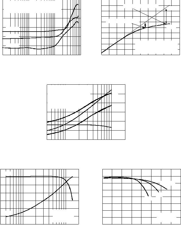
Figure 7. Intermodulation Distortion Products
versus Tone Spacing
1 10010
?60
0
0.1
7th Order
TWO?TONE SPACING (MHz)
VDD
= 28 Vdc, P
out
= 100 W (PEP), I
DQ
= 900 mA
Two?Tone Measurements
(f1 + f2)/2 = Center Frequency of 1960 MHz
5th Order
3rd Order
?10
?30
?40
?50
Figure 8. Pulsed CW Output Power versus
Input Power
Figure 9. 2-Carrier N-CDMA ACPR, IM3, Power Gain
and Drain Efficiency versus Output Power
0 ?70
Pout, OUTPUT POWER (WATTS) AVG.
60
?10
50
?20
40
?30
30
?40
10
?60
4 20010 100
?50
20
VDD= 28 Vdc, IDQ
= 900 mA
f1 = 1958.75 MHz, f2 = 1961.25 MHz
2?Carrier N?CDMA, 2.5 MHz Carrier
Spacing, 1.2288 MHz Channel
Bandwidth, PAR = 9.8 dB
@ 0.01% Probability (CCDF)
40
56
31
P3dB = 51.56 dBm (143.2 W)
Pin, INPUT POWER (dBm)
VDD
= 28 Vdc, I
DQ
= 900 mA
Pulsed CW, 8 μsec(on), 1
msec(off)
f = 1960 MHz
54
53
52
46
32 33 36 3734 35 38 39
Actual
Ideal
P1dB = 50.9 dBm (124.2 W)
55
48
30
10
17
0
70
Pout, OUTPUT POWER (WATTS) CW
Figure 10. Power Gain and Drain Efficiency
versus CW Output Power
VDD
= 28 Vdc
IDQ
= 900 mA
f = 1960 MHz
3 200100
10
16
15
13
12
11
60
40
30
20
10
Figure 11. Power Gain versus Output Power
Pout, OUTPUT POWER (WATTS) CW
VDD
= 32 V
IM3
ηD
Gps
ACPR
η
D
, DRAIN EFFICIENCY (%), G
ps
, POWER GAIN (dB)
IMD, INTERMODULATION DISTORTION (dBc)
IM3 (dBc), ACPR (dBc)
η
D
,
DRAIN EFFICIENCY (%)
Gps
ηD
G
ps
, POWER GAIN (dB)
200
6
18
0
16.5
10.5
9
25
12
15
28 V
IDQ
= 900 mA
f = 1960 MHz
P
out
, OUTPUT POWER (dBm)
G
ps
, POWER GAIN (dB)
?20
51
24 V
50
47
49
14
50
13.5
7.5
50 75 100 125 150 175


发布紧急采购,3分钟左右您将得到回复。
相关PDF资料
MRF6S19120HSR5
MOSFET RF N-CHAN 28V 19W NI-780S
MRF6S19140HSR5
MOSFET RF N-CHAN 28V 29W NI-880S
MRF6S19200HSR5
MOSFET RF N-CH 56W 28V NI780S
MRF6S20010GNR1
MOSFT RF N-CH 28V 10W TO270-2 GW
MRF6S21050LSR5
MOSFET RF N-CH 28V 11.5W NI-400S
MRF6S21060NR1
MOSFET RF N-CH 28V 14W TO270-4
MRF6S21100HSR5
MOSFET RF N-CHAN 28V 23W NI-780S
MRF6S21100NR1
MOSFET RF N-CH 28V 23W TO270-4
相关代理商/技术参数
MRF6S19100MBR1
功能描述:MOSFET RF N-CH 28V 22W TO272-4 RoHS:否 类别:分离式半导体产品 >> RF FET 系列:- 产品目录绘图:MOSFET SOT-23-3 Pkg 标准包装:3,000 系列:- 晶体管类型:N 通道 JFET 频率:- 增益:- 电压 - 测试:- 额定电流:30mA 噪音数据:- 电流 - 测试:- 功率 - 输出:- 电压 - 额定:25V 封装/外壳:TO-236-3,SC-59,SOT-23-3 供应商设备封装:SOT-23-3(TO-236) 包装:带卷 (TR) 产品目录页面:1558 (CN2011-ZH PDF) 其它名称:MMBFJ309LT1GOSMMBFJ309LT1GOS-NDMMBFJ309LT1GOSTR
MRF6S19100MR1
功能描述:MOSFET RF N-CH 28V 22W TO270-4 RoHS:否 类别:分离式半导体产品 >> RF FET 系列:- 产品目录绘图:MOSFET SOT-23-3 Pkg 标准包装:3,000 系列:- 晶体管类型:N 通道 JFET 频率:- 增益:- 电压 - 测试:- 额定电流:30mA 噪音数据:- 电流 - 测试:- 功率 - 输出:- 电压 - 额定:25V 封装/外壳:TO-236-3,SC-59,SOT-23-3 供应商设备封装:SOT-23-3(TO-236) 包装:带卷 (TR) 产品目录页面:1558 (CN2011-ZH PDF) 其它名称:MMBFJ309LT1GOSMMBFJ309LT1GOS-NDMMBFJ309LT1GOSTR
MRF6S19100N
制造商:Freescale Semiconductor 功能描述:
MRF6S19100NBR1
功能描述:射频MOSFET电源晶体管 1990MHZ 22W RoHS:否 制造商:Freescale Semiconductor 配置:Single 晶体管极性: 频率:1800 MHz to 2000 MHz 增益:27 dB 输出功率:100 W 汲极/源极击穿电压: 漏极连续电流: 闸/源击穿电压: 最大工作温度: 封装 / 箱体:NI-780-4 封装:Tray
MRF6S19100NR1
功能描述:射频MOSFET电源晶体管 1990MHZ 22W RoHS:否 制造商:Freescale Semiconductor 配置:Single 晶体管极性: 频率:1800 MHz to 2000 MHz 增益:27 dB 输出功率:100 W 汲极/源极击穿电压: 漏极连续电流: 闸/源击穿电压: 最大工作温度: 封装 / 箱体:NI-780-4 封装:Tray
MRF6S19120H
制造商:FREESCALE 制造商全称:Freescale Semiconductor, Inc 功能描述:RF Power Field Effect Transistors
MRF6S19120HR3
功能描述:射频MOSFET电源晶体管 HV6 19W N-CDMA RoHS:否 制造商:Freescale Semiconductor 配置:Single 晶体管极性: 频率:1800 MHz to 2000 MHz 增益:27 dB 输出功率:100 W 汲极/源极击穿电压: 漏极连续电流: 闸/源击穿电压: 最大工作温度: 封装 / 箱体:NI-780-4 封装:Tray
MRF6S19120HR5
功能描述:射频MOSFET电源晶体管 HV6 19W N-CDMA RoHS:否 制造商:Freescale Semiconductor 配置:Single 晶体管极性: 频率:1800 MHz to 2000 MHz 增益:27 dB 输出功率:100 W 汲极/源极击穿电压: 漏极连续电流: 闸/源击穿电压: 最大工作温度: 封装 / 箱体:NI-780-4 封装:Tray
